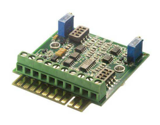
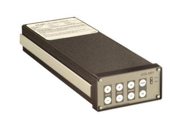
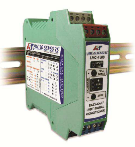
In the 1990s, the sensor and micro electronic recorder group as one of the storage test products in the international emergence. Storage test technology is a new method of testing parameters on the bullet from the seventies, it is a dynamic test technology that does not affect the object under test or affect the conditions in the permissible range, micro data acquisition and storage tester is placed in the body under test, the rapid collection and memory of information is completed in real time on site, and the recorder is recovered afterwards, and the test information is processed and reproduced by the computer. The electronic pressure tester is a typical product of the storage test technology, which is used to measure the bore pressure parameters within the bore pressure, and the dynamic pressure parameters are an important basis for evaluating the ballistic performance of artillery, powder charges, projectiles and fuses, etc.
Design of Signal Conditioning Circuits
The role of signal conditioning circuits in voltage measurement systems
The purpose of signal conditioning is to facilitate the transmission and processing of signals, and its role can be summarized in the following three points:
a) The charge signal output from the sensor is to be converted into an electrical signal that can be processed by the subsequent circuit.
b) The electrical signal output from the sensor is very weak, and most of it cannot be directly delivered to the recording instrument, so a preamplifier is needed to amplify the electrical signal.
c) The electrical signal is mixed with interference noise, and a filter circuit is required in the detection circuit, with the purpose of removing various interferences mixed in the useful signal,
improving the signal-to-noise ratio by eliminating noise, and compensating and correcting the zero position error and gain error.
Balancing circuit
Due to the initial resistance value of the bridge resistor is not exactly the same, plus the stringing in of the connecting wire resistance, there is an initial imbalance in the bridge when the strain is not felt, which will occupy the dynamic range of the instrument if it is too serious and affect the normal operation of the instrument. In addition to linear amplification of weak signals, the instrumentation amplifier is also tasked with matching and anti-common-mode interference. Therefore, the instrumentation amplifier is required to have high common-mode rejection ratio, high speed, wide bandwidth, high accuracy, high input impedance, low output impedance, and low noise.
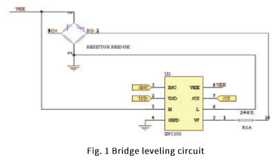
The auto-leveling circuit consists of the X9C103, a full-bridge circuit, and an additional appropriate gate circuit.
The strain measurement bridge designed in this paper consists of a working resistive strain gauge, a temperature compensated resistive strain gauge and two precision resistors of equal resistance to the selected resistive strain gauge. However, since the initial resistance values of these four resistors are not exactly the same, plus the need to connect the strain gauges to the measurement circuit with wires, the resistance of the wires is also part of the bridge arm resistance because of the existence of a certain resistance of the wires themselves, and because it is connected in series with the resistance strain gauges on the bridge arm of the measurement circuit, but it does not participate in the deformation itself. When the strain is not felt, it makes the bridge have an initial imbalance. If this initial imbalance is too severe, there will be some error in the measurement results. In order to improve the measurement accuracy, it is necessary to correct for the initial resistance and the error caused by the wire.
The resistor balancing adjustment circuit is shown in Figure 1.
As shown in Figure 1, the balancing circuit consists of a fixed resistor Rb and a potentiometer Ra. Its center tap divides Ra into two parts, xRa and (1-x)Ra. As shown in Figure 2, x can vary from 0 to 1, and when x=0 the tap of the potentiometer is connected to point C, making Rb and R2 in parallel. When x=1, the tap of the potentiometer is connected to point A, making Rb and R1 in parallel.
Instrumentation amplifier circuits
In most instruments and measuring devices, the output of the bridge is connected to the input of the amplifier, as the input impedance of modern integrated amplifiers is often above 10 MΩ. In this connection, the output current of the bridge is so small as to be negligible, and the output of the bridge can be considered to be open diagonally.
The strain measurement amplifier circuit designed in this paper uses the INA128 from TI, which is a low-voltage general-purpose instrumentation amplifier. With its excellent characteristics, small size, and the ability to easily set the gain from 1 to 10,000 with an external resistor, the INA128 can be used in a wide range of applications such as signal acquisition and amplification, medical instrumentation, and multi-channel systems, and is ideal for portable and other battery-powered systems because it can operate at supply voltages as low as ±2.25V and has a low quiescent operating current.
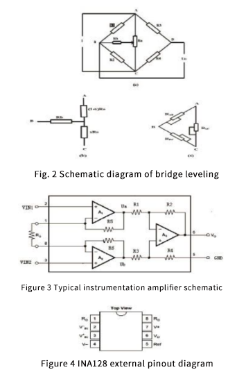
The amplifier consists of two stages connected in series. The front stage is two homogeneous amplifiers with symmetrical structure, and the input signals are added to the homogeneous inputs of A1 and A2, thus having high capability of common mode interference suppression and high input impedance. The rear stage is a differential amplifier, which not only cuts off the transmission of common-mode interference, but also transforms the double-ended input mode into a single-ended output mode, adapting to the needs of ground load.
The INA128 is laser etched, has a low threshold voltage (50μV/°C) and high attenuation in conventional mode, and a low supply voltage, down to a supply quiescent current of only 700A, so it is ideal for battery power. Internal input protection is available within 40V without damage.
The internal structure of the INA128 is shown in Figure 5.
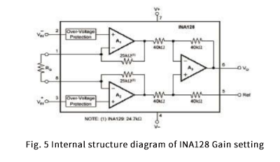
The amplification that can be obtained with an independent external resistor RG in the basic connection of INA128 is: G=1+50kΩ/RG.
Where 50kΩ is the sum of the two amplifier feedback resistors inside the INA128, which are laser-corrected for high accuracy and small temperature coefficient, and whose influence is already included in the device performance given in the manual. The accuracy and temperature stability of the external resistors directly affects the gain, especially for larger gains (G ≥ 100), and the resistance of the connecting wires and jacks can also introduce additional errors in the gain. In other words, the RG value in the equation should be the sum of external resistance and stray resistances such as connecting wires.
Noise Interference
The internal noise of INA128 is very small, when G≥100, the output voltage signal of low frequency noise from 0.1Hz to 10Hz is only about 0.2μVp-p, which is much smaller than the current low noise chopper amplifier. To reduce the impact of external interference and power supply noise, a decoupling capacitor should be connected immediately adjacent to the power supply pin.
Out-of-Sync Compensation
The INA128 is laser-corrected so that both out-of-tune and temperature drift are small and do not require adjustment in most cases, and the circuit can be externally compensated if necessary. The addition of a voltage follower isolates the zeroing circuit from the instrumentation amplifier, maintaining the low impedance of pin Ref and ensuring good common-mode rejection of the amplifier.
Common-mode input signal range
If the common-mode voltage in the input signal is too large, it will saturate the input amplifier. At critical saturation, the output voltage of VO is VO = VCM - VO/2. The linear input range of the INA128 extends from approximately -1.7 V to +1.4 V from the supply. For a defined supply voltage, the larger the output voltage Vo, the smaller the allowed common-mode signal.
Low voltage operation
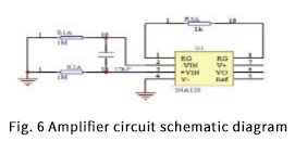
The INA128 is characterized by a wide range of applicable supply voltages. Most parameters maintain good performance when the supply voltage varies from ±2.25V to ±18V, as shown in the circuit in Figure 6.
Filter circuit design
After the pressure sensor signal passes through the balancing circuit and the instrumentation amplifier, it is often necessary to filter the signal to remove the noise interference superimposed in the signal in order to achieve a more ideal measurement effect. In this paper, we plan to use a second-order voltage controlled low-pass filter to filter the pressure sensor signal. The signal picked up by the measurement system from the sensor often contains noise and many signals unrelated to the measured, and the original measurement signal is transmitted, amplified, exchanged, arithmetic and various other processing processes, also mixed with a variety of different noise, thus affecting the accuracy of the measurement. These noises are generally very random and difficult to be distributed in a specific frequency band in the frequency domain. Signal separation circuits generally use filters to achieve the suppression of noise from the frequency domain and extract the required measurement signal, which is a necessary component of various measurement systems. In the actual test system, if we are required to amplify a weak small signal, some interference signals are amplified at the same time, which seriously affects the quality of our test, therefore, the original signal needs to be pre-processed. Pre-filter circuit (anti-alias filter) is a common means for us to weaken the noise. The main function of the filter is to allow the specified frequency band signal can pass more smoothly, while the other frequency band signal to play a role in attenuation. In the test of high impact field, the pre-processing needs to suppress mainly high frequency signals to avoid the signal spectrum overlap at a certain sampling frequency. Need to design a low-pass filter to pre-processing. The role of the low-pass filter is to make the high-frequency signal as much as possible to attenuate, while allowing the useful low-frequency signal to pass smoothly.
Types of Filters
Filters can be divided into two categories: analog and digital, depending on the form of the signal being processed. There are many similarities between the two in terms of functional characteristics, but there are significant differences in terms of structural composition. The former process continuous analog signals, while the latter are discrete digital signals.
Filters have three different selective effects on signals of different frequencies:
(1) In the passband the signal is attenuated by a small amount and passed.
(2) The signal is suppressed by a large attenuation in the blocking band.
(3) The transition band between the passband and the stopband is subject to varying degrees of attenuation.
Filters for different frequency bands in the full frequency band distribution of different positions, can achieve the role of the selection of different frequency signals. According to the selected frequency filter four types namely: high-pass, low-pass, band-pass, band-stop. In addition there is an all-pass filter, a variety of signals are able to pass, but the phase has no change, he is actually a phase shifter. According to the composition of the circuit can be divided into LC passive filter, RC passive filter, LC active filter and RC active filter. According to the transfer function can be divided into first-order filter, second-order filter and high-order filter.
Introduction of Power Supply Circuit and Simulation of Signal Conditioning Circuit
In order to make the Wheatstone bridge in the pressure sensor work properly, we need to provide a relatively accurate power supply, and its ripple voltage must be very small.
The role of power supply circuit
Power control technology is the key technology to achieve low power consumption in electronic test instruments. In short, that is, the circuit is powered up when it needs to work, and powered down when it does not need to work, reducing the proportion of power consumption when the circuit is not operating effectively. At this time, the system has a variety of power supply, the use of a single battery power supply to achieve multi-branch power network management, so that the power supply of each functional module of the system is relatively independent power supply, when not working can be powered off separately to save power consumption, but at this time need to pay attention to the compatibility of the charged part and uncharged part of the problem.
Power supply chip selection
The more commonly used power supply chips are 7325, 7333, 7350, AD587, etc. These power supply chips are capable of outputting stable 2.5V, 3.3V, 5V, 10V voltages respectively, and through the design of bypass capacitors, their ripple voltages are smaller and more suitable for power control circuits.
The bridge must be powered by a constant voltage supply to ensure that the supply voltage remains highly stable in the event of changes in the sampling frequency, load, and many other external environments, which is difficult to achieve in practice without the use of a dedicated regulated power supply, so the LP2987 is used as the dedicated power supply in this design.
Design and Simulation of Signal Conditioning Circuits
The process of simulation can be divided into the following steps:
1. data input: the structure of the circuit diagram created by the user, the component data are read in and the analysis method is selected;
2. Parameter setting: The program checks the structure and nature of the input data, and the parameters set by what is elaborated in the circuit.
3. Circuit analysis: The input signal is analyzed, and it is the key to the circuit simulation. It will form the numerical solution of the circuit and send the resulting data to the output pole.
4. Data output: The simulation run results are obtained from test instruments such as oscilloscopes and other up points. and analyze it.
In this paper, based on the analysis of the development status of pressure testing systems at home and abroad, the leveling circuit, signal amplification circuit, filter circuit and power supply circuit of the bridge are designed for the resistive strain gauge pressure sensor. The output signal of the pressure sensor is very weak, difficult to measure and analyze, and the test result error is large. It is of theoretical value and practical significance to design the signal leveling circuit and constant voltage power supply circuit of the pressure sensor to obtain a stable, amplified and undistorted output signal.The X9C103, full-bridge circuit and additional appropriate gate circuit are used to form the auto-leveling circuit; the INA128 instrumentation amplifier is used to form the amplifier circuit; the OPA340 amplifier is used to form the second-order low-pass filter; and the dedicated power supply chip is used to form the constant-voltage power supply circuit. The circuit design was implemented using Protel dedicated circuit design software, and the signal conditioning circuit was simulated using EWB circuit simulation software. The simulation results show that the amplifier circuit achieves 100 times signal amplification, and the cut-off frequency of the low-pass filter circuit is 159Hz, which is the same as the theoretical value, thus verifying the correctness of the design. The circuit is simulated by integrating each module to realize the leveling, filtering and power control of the pressure sensor, and drawing the schematic diagram.


